

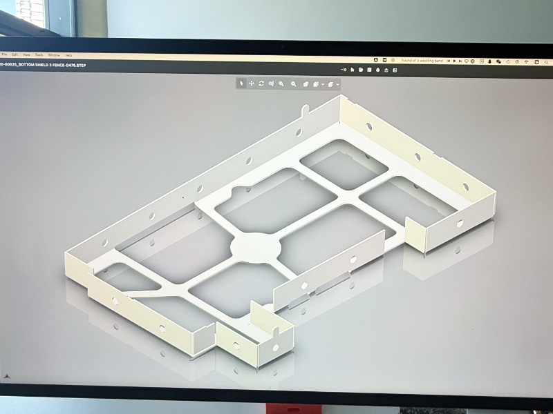
Single-Piece Shielding Can FOR PCB
Compact, cost-effective, and easy-to-assemble solution for high-density designs.
What Is a Single-Piece Shielding Can?
A single-piece shielding can—also called a one-piece shield—is a precision-stamped metal enclosure designed to provide EMI/RFI protection for sensitive PCB components.
Unlike the two-piece (frame-and-lid) structure, it is formed from a single sheet of metal, with continuous sidewalls that are directly soldered to the PCB pads during SMT or reflow.
This simplified construction offers excellent dimensional stability, lower production cost, and faster assembly, making it ideal for high-volume, cost-sensitive designs or modules where no frequent internal probing is required.
It is commonly applied in Wi-Fi modules, IoT devices, automotive electronics, set-top boxes, and industrial control units, ensuring consistent EMI suppression and compact form-factor integration.
Thickness
0.2–0.4 mm
Flatness
±0.02mm
Tolerance
±0.05mm
Why Choose Single-Piece Shields
Single-piece shielding cans are designed to deliver reliable EMI/RFI protection with the best balance of performance, cost, and assembly efficiency. Their one-piece construction eliminates the need for separate frames or covers, reducing tooling complexity and assembly time while maintaining excellent mechanical strength and flatness.
Cost-Effective Manufacturing
The one-piece design simplifies stamping and minimizes tooling stages, resulting in lower per-unit cost and shorter lead time—ideal for large-volume production.
Fast & Easy Assembly
The shield can be soldered directly to PCB pads during standard SMT or reflow processes, saving assembly steps and ensuring strong electrical grounding
Compact & Space-Saving
Without a frame-lid structure, the overall height and footprint are reduced—perfect for high-density layouts or low-profile modules such as Wi-Fi and IoT boards.
Fully Customizable
Available in various materials (nickel silver, SPTE, stainless steel), thicknesses (0.15–0.4 mm), and surface finishes (tin, nickel, gold, passivation). Optional embossing, holes, or positioning legs can be added to meet design needs.
Specifications & Custom Options
Each single-piece shielding can is fully customizable to meet your PCB design and functional requirements.
We offer a wide range of materials, thicknesses, heights, and surface finishes to ensure optimal EMI performance and compatibility with different soldering processes.
Optional features such as vent holes, embossing ribs, and positioning legs are available to enhance heat dissipation, rigidity, and alignment accuracy.
- Material: C7701 / C7521 Nickel Silver, SPTE, SUS304
- Thickness :0.05 – 0.80 mm
- Surface Finish:Tin, Nickel, Gold, Silver, Passivation
- Vent / Hole :Custom openings, <1 mm holes, 10–30 % open area
- Features:Embossed ribs, positioning legs, test holes
- Tolerance: ±0.05 mm (dimension), Flatness ≤0.05 mm
- Packaging :Reel & Tape / Tray / Blister
Design & Pad Guidelines
- Extend solder pads slightly beyond the shield wall to provide adequate solder volume and mechanical strength.
- Keep solder mask openings aligned with pad edges for clean solder flow and easy inspection.
- Avoid placing high components too close to the shield area to prevent solder shadowing.
- Vent holes or slots can help with heat dissipation and pressure balance during reflow.
- Keep the total open area below 30 % to maintain effective EMI/RFI attenuation.
- For frequencies above 1 GHz, use smaller holes (< 1 mm) and continuous wall spacing to avoid leakage.
- If in-circuit testing is required, add small test holes or removable windows.
- Consider using narrow slits instead of large cutouts to minimize EMI leakage.
- Maintain shield flatness within ≤ 0.10 mm for prototypes and ≤ 0.08 mm for mass production.
- Use embossed ribs or post-forming flattening to enhance rigidity and control deformation.
- Compatible with standard SMT and reflow soldering processes.
- Follow a gradual heating curve to prevent warping or oxidation.
- Ensure sufficient stencil aperture to achieve full solder wetting along the shield perimeter.
Reliability & Quality
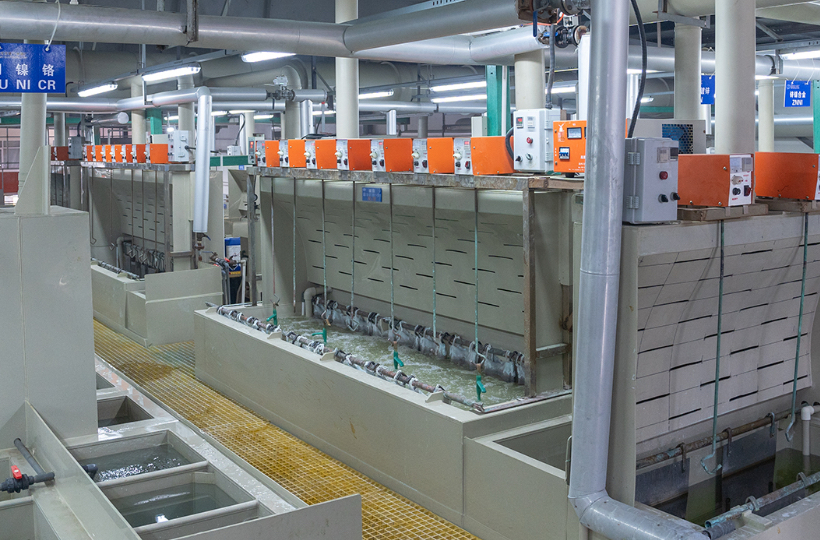
Our electroplating process includes surface cleaning, controlled plating, inspection, and safe packaging.
Each step is carefully managed to ensure uniform coating thickness, strong adhesion, and reliable appearance quality.
- All products are fully compliant with RoHS and REACH environmental standards.
Salt Spray Corrosion Test
Verify anti-corrosion performance
Solderability Test
Ensure strong and clean solder joints
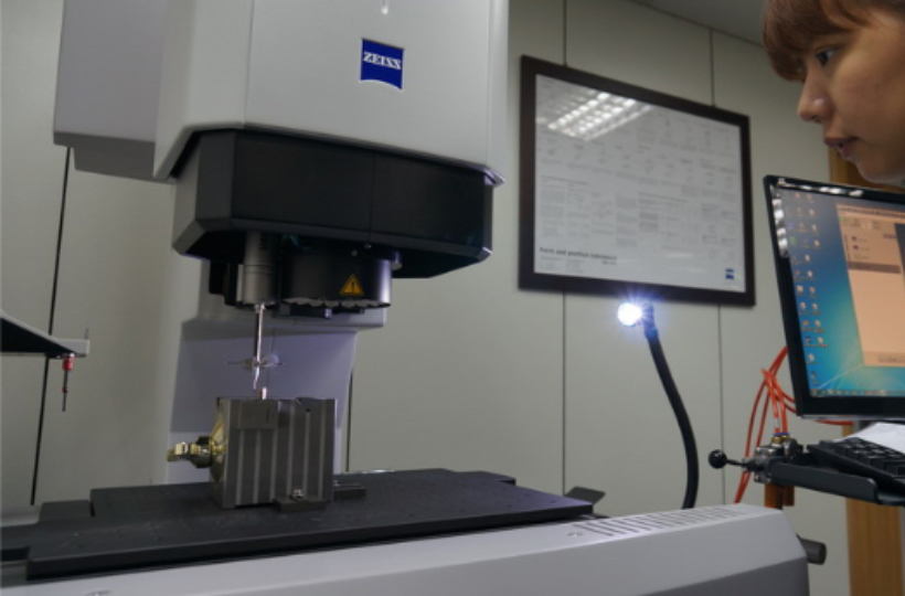
Microscopic Burr Inspection
Detects tiny burrs and surface defects to guarantee precision finishing
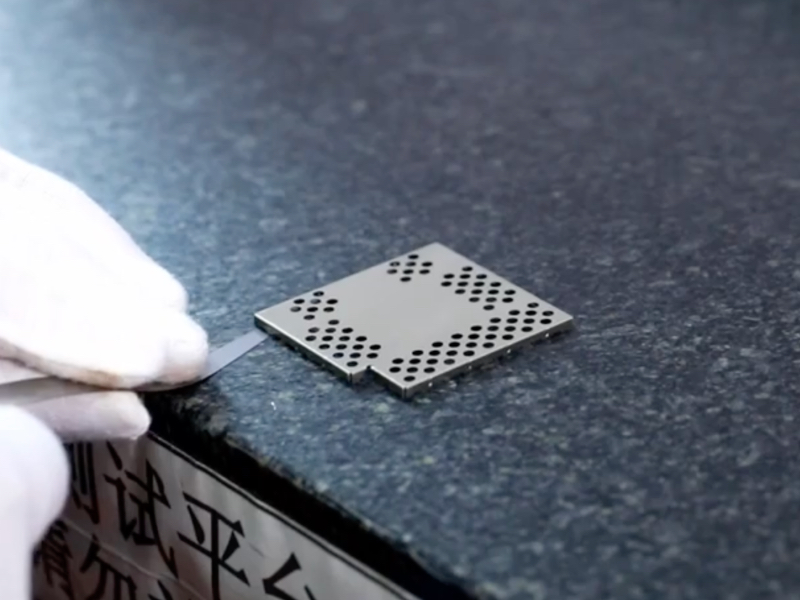
Flatness Measurement
Ensures even solder contact and mechanical stability
Typical Applications
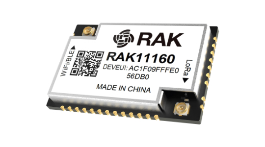
Wi-Fi module shielding system
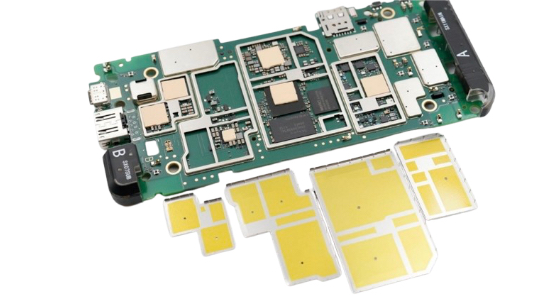
Two-piece shield structure
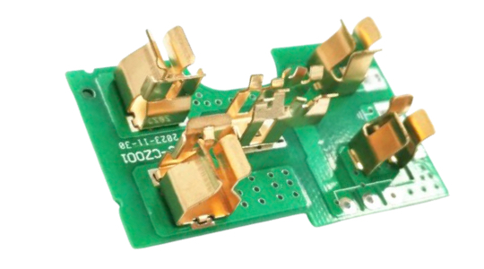
Spring contact for antenna grounding
Production & Delivery

Submit Drawing or Sample
Upload your PCB drawing (STEP, DXF, or PDF) or send a physical sample. Our engineers will evaluate manufacturability, material selection, and cost optimization.
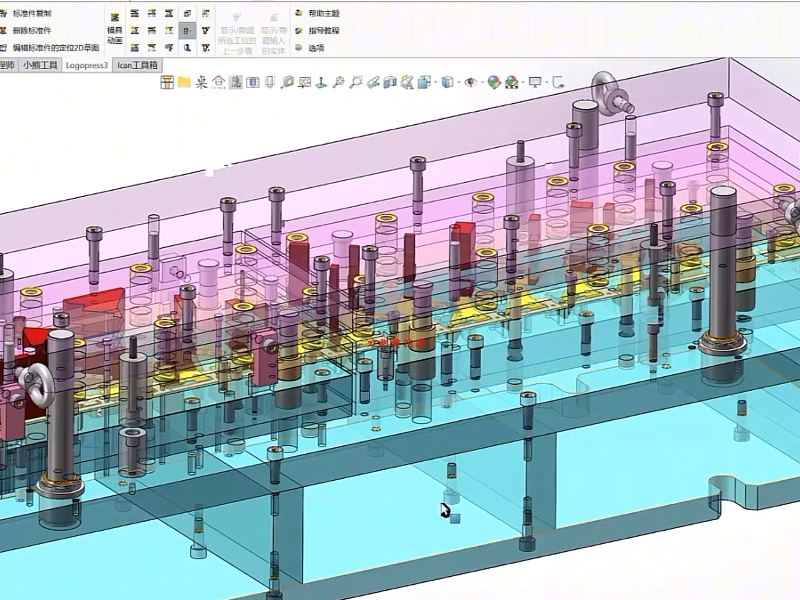
Engineering Review (24 h Quote)
Within 24 hours, you’ll receive a detailed quotation with material options, tooling costs, and lead time. We confirm feasibility and provide suggestions for flatness or structure improvement if needed.

Tooling / Prototype (3–7 Days)
Rapid prototype tooling and stamping are completed within 3–7 working days. Samples are produced, inspected, and packed for your functional or fit validation.

Inspection & Approval
Every prototype is measured for flatness, dimension, and plating quality. We provide inspection reports and photos for your approval before mass production.
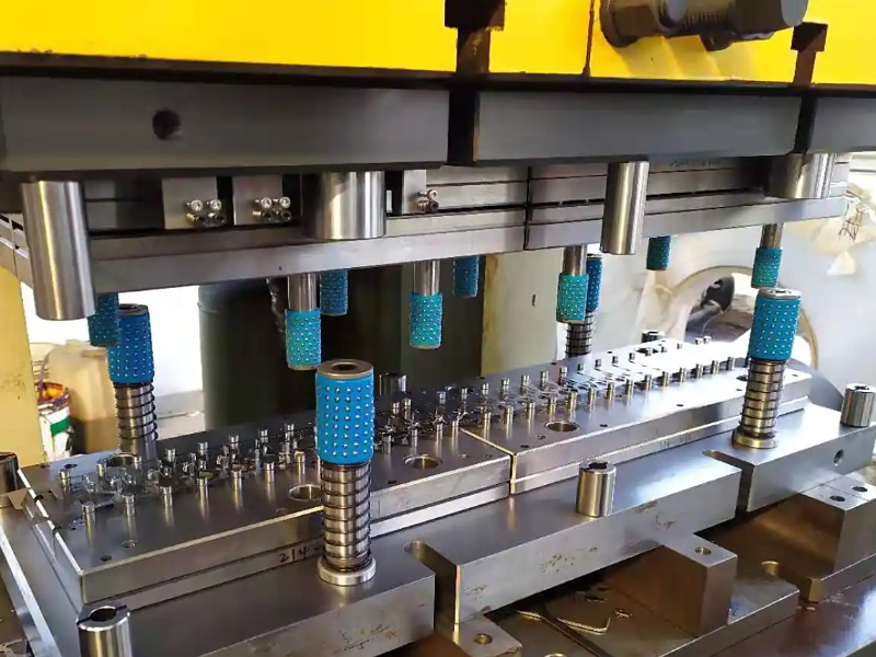
Mass Production (15–20 Days)
Once approved, full production begins with stable tooling and SPC process control. Consistent quality, packaging, and labeling are maintained for each batch.
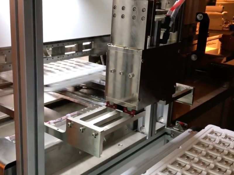
Packaging & Shipment
Finished goods are vacuum-packed or blister-packed with desiccants and anti-collision protection. Shipments are arranged via DHL, UPS, or your preferred forwarder under EXW or CIF terms.
we’re here to all your questios
Have questions about our shielding cans? Explore the most common topics our engineers get asked — fast, clear, and practical answers all in one place.
When should I choose single-piece vs. two-piece?
Choose a single-piece shield when cost, compact size, and fast SMT assembly are the priorities.
It’s ideal for high-volume production where internal debugging or rework is rare.
A two-piece shield (frame + lid) is better when you need frequent access to the circuit for tuning or testing, even though it adds cost, height, and assembly steps.
Can holes reduce EMI shielding effectiveness?
Yes. Openings create potential leakage paths for high-frequency signals.
To maintain effective shielding, keep the total open area below 30 percent and use small holes (typically < 1 mm for > 1 GHz applications).
Distribute holes evenly and avoid long slots to prevent concentrated leakage.
Can selective plating be done?
Yes. Selective plating such as nickel-gold, nickel-tin, or localized gold pads is available.
This allows certain areas to have higher conductivity or solderability while keeping overall cost under control.
Selective plating usually requires a higher minimum order and slightly longer lead time.
How do you control flatness during production?
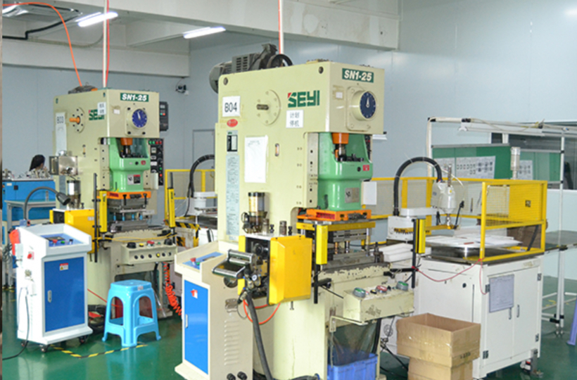
Flatness is controlled through careful material selection, optimized stamping and forming, and post-process leveling or embossing.
We inspect each batch with optical and mechanical gauges.
Typical tolerance: ≤ 0.10 mm for prototypes and ≤ 0.07 mm for mass production, ensuring stable reflow soldering and contact.
How do you protect from oxidation during shipping?
All parts are made from pre-plated or corrosion-resistant materials and handled with gloves.
They are vacuum-sealed or packed in moisture-proof bags with desiccants and humidity indicators, then boxed with anti-collision protection.
For best results, store below 25 °C and 60 % RH; typical shelf life is 6–12 months depending on finish type.
Hexin Electronics — From concept to completion, we make precision happen.
Hexin
Rapid Prototyping & Sampling
Precision Tooling Design & Manufacturing
Mass Production
Surface Finishing & Plating
Quality Inspection & Reliability Testing
Custom Packaging & Global Delivery
Related Products
Get a Fast Quote in 24 Hours
Thickness
0.2–0.4 mm
Flatness
±0.02mm
Tolerance
±0.05mm