
Hexin

Through-Hole Spring Contacts

Robust PCB Connection for Grounding, Shielding, and Structural Support

Surface Mount Spring Contacts
Through-Hole Spring Contacts

What Are Through-Hole Spring Contacts?

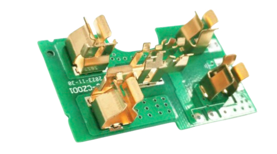
Through-hole spring contacts (THT spring contacts) feature a tail or pin structure that passes through the PCB hole and is soldered to create a firm mechanical and electrical joint.

This configuration enables greater compression range, higher spring force, and improved retention, making them suitable for heavy-duty environments or larger shield connections.

Common Materials: Phosphor Bronze, Beryllium Copper, Stainless Steel

Finishes Available: Tin, Nickel, or Gold — all RoHS & REACH compliant

Thickness

0.2–1.0 mm

Flatness

±0.02mm

Tolerance

±0.05mm

Key Features & Advantages

Designed for performance and strength, Hexin through-hole spring contacts offer outstanding reliability in demanding PCB assemblies:

High Retention Strength

Firmly anchored through plated holes for vibration-resistant mounting.

High Spring Force & Travel

Supports larger compression distances for shield lids or multi-point grounding.

Low Contact Resistance

Maintains excellent conductivity throughout the product’s life cycle.

Superior Durability

Resistant to thermal stress during wave soldering and reflow processes.

Specifications & Custom Options

Our through-hole spring contacts are available in various heights, forces, and plating finishes to meet different mechanical and electrical requirements.

Custom designs can be tailored for pin length, compression range, and plating material to perfectly match your PCB assembly and performance needs.

6/5

Dr. Mr xie

engineer

15 years experienc

Design & Pad Guidelines


  • Recommended hole size should be 0.05–0.10 mm larger than the contact pin diameter for smooth insertion.

  • Maintain roundness tolerance within ±0.03 mm to ensure proper fit and solder flow.

  • Oversized holes may cause poor retention or misalignment during soldering.


  • Use plated-through holes (PTH) with copper plating thickness between 25–40 μm.

  • Ensure uniform plating for stable contact resistance and solder adhesion.

  • Avoid over-etching or uneven plating which could affect pin seating depth.


  • Standard board thickness: 1.0–1.6 mm FR-4 for most applications.

  • For thinner PCBs, adjust tail length or add mechanical reinforcement if needed.

  • Verify that the pin extends 0.5–1.0 mm beyond the bottom surface for proper solder coverage.


  • Suitable for wave soldering, selective soldering, or manual soldering operations.

  • Recommended solder alloys: Sn-Ag-Cu or Sn-Pb types.

  • Maintain sufficient solder volume to cover the entire hole wall and contact tail.

  • Avoid excessive heat that could reduce spring hardness or plating integrity.


  • Design for a working deflection of 0.5–1.0 mm to ensure stable contact pressure.

  • Maintain at least 0.5 mm clearance between the contact top and mating part after full compression.

  • Ensure the spring is not overstressed during assembly or cover installation.


  • The annular ring around the through-hole should be ≥0.2 mm wider than the drill diameter.

  • Use solder mask clearance of 0.05–0.1 mm around the pad to ensure clean solder joints.

  • Keep sufficient land area for AOI inspection and mechanical strength.


  • For large or heavy shields, consider adding mechanical fixing points or support brackets.

  • Avoid excessive board flexing or lateral stress during installation.

  • For automated insertion, ensure consistent pin alignment and feeding direction.


  • After soldering, perform visual or AOI inspection to verify full solder fill and no voids.

  • Check pin coplanarity and compression height consistency across all contacts.

  • Conduct continuity and resistance testing to ensure stable performance before final assembly.


Reliability & Quality

Our electroplating process includes surface cleaning, controlled plating, inspection, and safe packaging.

Each step is carefully managed to ensure uniform coating thickness, strong adhesion, and reliable appearance quality.

Salt Spray Corrosion Test

Salt Spray Corrosion Test

Verify anti-corrosion performance

Solderability Test

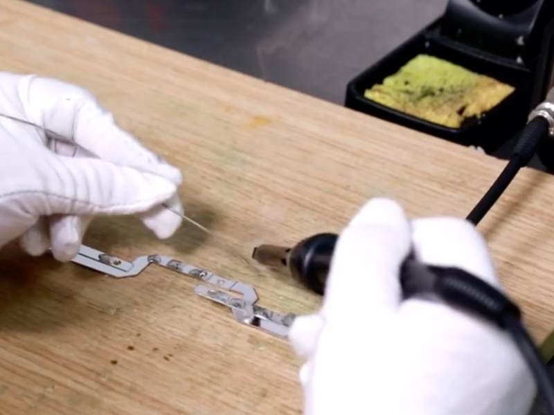
Solderability Test

Ensure strong and clean solder joints

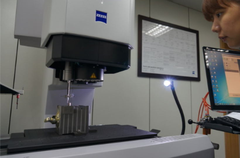
Microscopic Burr Inspection

Microscopic Burr Inspection

Detects tiny burrs and surface defects to guarantee precision finishing

Flatness Measurement

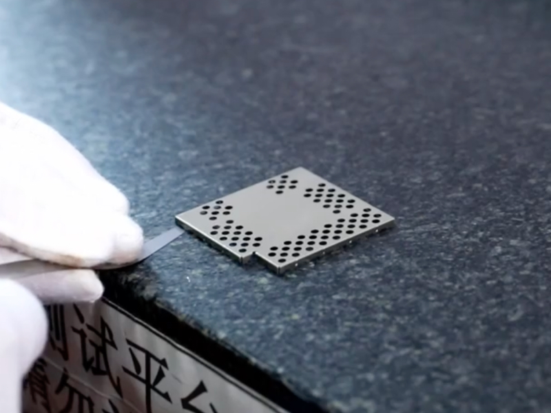
Flatness Measurement

Ensures even solder contact and mechanical stability

Typical Applications

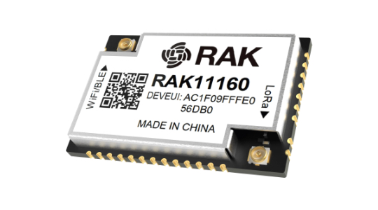
Wi-Fi module shielding system

Wi-Fi module shielding system

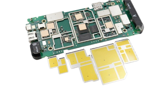
Two-piece shield structure

Spring contact for antenna grounding

Spring contact for antenna grounding

Production & Delivery

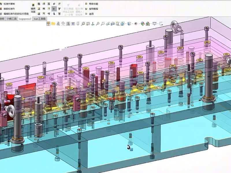
SPRING CONTACT TOOLING

Submit Drawing or Sample

Upload your PCB drawing (STEP, DXF, or PDF) or send a physical sample. Our engineers will evaluate manufacturability, material selection, and cost optimization.
Engineering Review (24 h Quote)

Within 24 hours, you’ll receive a detailed quotation with material options, tooling costs, and lead time. We confirm feasibility and provide suggestions for flatness or structure improvement if needed.

Rapid Prototyping

Tooling / Prototype (3–7 Days)

Rapid prototype tooling and stamping are completed within 3–7 working days. Samples are produced, inspected, and packed for your functional or fit validation.

Inspection & Approval

Every prototype is measured for flatness, dimension, and plating quality. We provide inspection reports and photos for your approval before mass production.
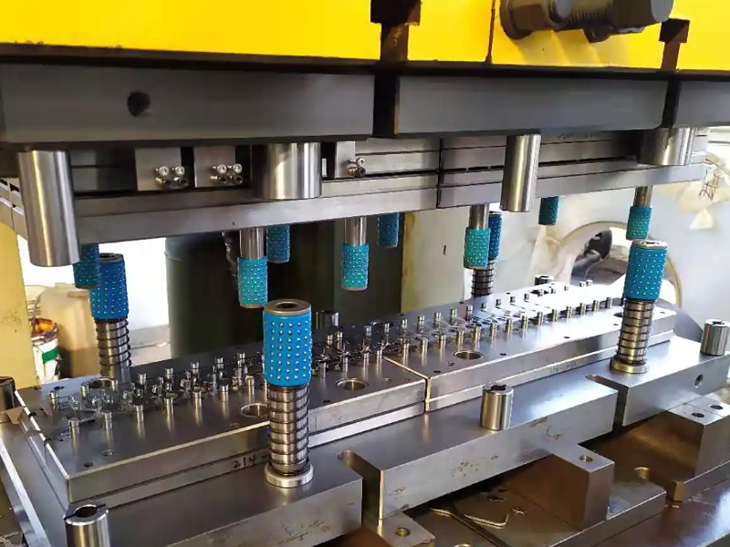
Mass Production (15–20 Days)

Once approved, full production begins with stable tooling and SPC process control. Consistent quality, packaging, and labeling are maintained for each batch.
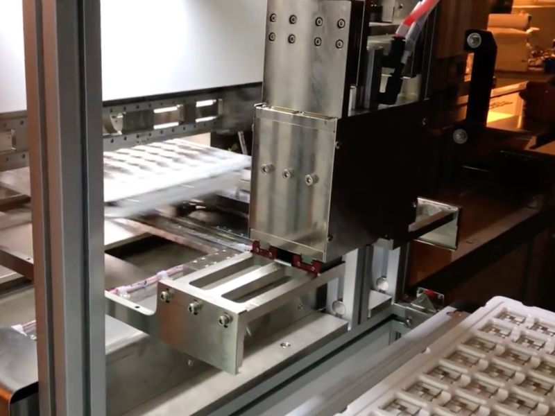
Packaging & Shipment

Finished goods are vacuum-packed or blister-packed with desiccants and anti-collision protection. Shipments are arranged via DHL, UPS, or your preferred forwarder under EXW or CIF terms.


MAKE EMI SPRING CONTACT

we’re here to all your questios

Find quick answers to common questions about the design, hole size, soldering method, and customization options of our through-hole spring contacts.

Through-hole versions provide stronger retention and can handle higher compression forces, ideal for large shields and mechanical stress environments.

Typically, the PCB hole should be 0.05–0.10 mm larger than the pin diameter for easy insertion and reliable soldering.

Yes, Hexin supports custom configurations for height, tail, spring force, and surface finish.

Absolutely — all through-hole spring contacts are designed to withstand wave soldering and manual solder repair.

Prototype tooling and samples: 3–7 working days

Mass production: 15–20 days depending on quantity and complexity.

Hexin Electronics — From concept to completion, we make precision happen.

Hexin

Rapid Prototyping

Rapid Prototyping & Sampling

We provide prototype samples within 1–3 days for quick design validation and performance testing, helping customers accelerate their R&D process.
Precision Tooling

Precision Tooling Design & Manufacturing

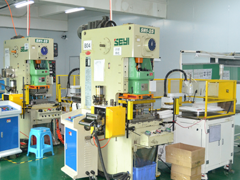
With in-house tooling facilities and experienced engineers, we develop high-precision stamping dies in 15–20 days, ensuring efficiency and long tool life.
Mass Production

Mass Production

Fully automated stamping, plating, and inspection processes guarantee stable output, high precision, and competitive pricing
Surface Finishing & Plating

Surface Finishing & Plating

Available finishes include nickel, tin, gold, silver, and passivation, improving corrosion resistance, conductivity, and solderability.
Quality Inspection

Quality Inspection & Reliability Testing

Each batch is tested for flatness, plating thickness, and solderability, ensuring compliance with IPC and customer standards.
Custom Packaging

Custom Packaging & Global Delivery

We offer reel & tape, blister tray, and vacuum packaging, along with reliable international logistics for timely and safe delivery.

Related Products

Single piece shielding can
A one-piece shielding can offers a compact, cost-effective EMI/RFI protection solution with fast SMT assembly and excellent dimensional stability.
Deep-Drawn Shield Can
Seamless Structure Formed By Precision Deep Drawing. Ideal For High-Frequency Or Hermetically Sealed Applications, Offering Excellent Strength, Dimensional Stability, And Smooth Surface Finish
SMT Spring contact
The surface-mount design allows direct reflow soldering onto PCB pads, eliminating the need for through-holes and enabling full compatibility with automated SMT processes.
Two-Piece Shielding Can
Frame-And-Lid Design For Modules Requiring Frequent Debugging Or Maintenance. Offers Easy Lid Removal, Excellent EMI Isolation, And High Reusability.

Get a Fast Quote in 24 Hours

Thickness

0.2–0.4 mm

Flatness

±0.02mm

Tolerance

±0.05mm

    Input this code: captcha